Overview
Application
Software
Additional Info
FAQ
Overview
Overview of features and benefits
Measurements
- Optical, non-contact, non-destructive
- High speed: Up to 100,000 3D point measurements per second
- Micron resolution, excellent S/N ratio
- 2D and 3D surface and subsurface characterization
- Dimensions, roughness, defects, thickness
- Long stroke profilometry
Imaging
- Surface profiles
- Cross-sections
- Volumetric images
Fiber-based probes
- Inspect inside bores, tubes, and crevices
- Provide versatility for high-speed online inspection
Benefits
- Wide range of materials: metal, plastics, polymers, glass, metal coatings, silicone, adhesives; reflective, transparent, semi-transparent, specular, nonspecular
- Wide range of surfaces: measured objects can be stationary or moving, solid or liquid, and include interiors of bores and tubes, exteriors of cylinders, concave or convex spherical shapes
- Small-diameter probes reach in to measure insides of bores and small-diameter tubes
- Measures high-aspect-ratio features: undercuts, cross-holes, chamfers, rifling, threads, O-ring grooves, and edges
- Reduced inspection cycle time: up to 100,000 measurements per second, each representing a 3D topographic point
- Versatility of setup: Non-contact probes work up to 1 m away from surface and several meters from the interferometer
- Continuous, long profile scanning: no area stitching required
- Flexible options for evaluating inspected parts: measured features can be compared to CAD drawings or to a user-defined set of locations, nominals, and tolerances
- Simple scan definition and execution: The scanning sequence is defined once by teaching the system with a joystick. The scanning sequence can later be executed with the push of a button.
- Time-saving automated reporting: Following a scan, go-no-go reports can be produced, and results logged in a manner compatible with industry-standard mechanisms
- Easily integrated in lab, shop, or fully-automated inspection setups: probes may be mounted on XY tables, on multi-axes scanning mechanisms, inside machining centers, above moving webs, on robot heads, etc.
- Adaptable to hostile environments: radioactive, very hot, cryogenic, vacuum, etc.
- No consumables are needed: Optical probes do not come in contact with the measured samples, and therefore do not wear out like contact probes
- USB connection for data transfer from interferometer to PC or laptop
- Option of multiplexing several probes with single interferometer for additional return on investment (ROI)
Application
Metrology Applications
Typical measurements
- Dimensional measurements: geometric dimensioning and tolerancing (GD&T) parameters
- Thickness: single-layer or multilayer films, coatings
- Surface roughness: surface characterization, flatness, and more
- Volume loss: component wear or other damage
- High-aspect-ratio features: steps, holes, grooves, channels
- Hard-to-reach spaces: interiors of bores, small aperture tubes, etc.
- Profilometry in hostile environments: radioactive, cryogenic, very hot
- Long stroke profiles
- Thickness of non-transparent materials
3D metrology and imaging for industry and R&D
- Quality control
- Online 3D production inspection, GD&T
- Statistical process control SPC
- R&D
Examples of applications
- Electronics industry: geometry measurements of CMP pad grooves, glass edge and thickness measurement, wafer geometry
- Aerospace: jet engine turbine vanes
- Automotive: drive shafts, axles, threads, splines, gears, drive teeth
- Medical instruments sector: tubes, implant shaft interiors, optical cross-sections of intra-ocular lenses
- Biomedical and chemical sectors: vials, IDs of cylindrical containers
- Defence industry: barrels, bores, reamers, mandrels, drill bits, die blocks
- Tubular parts in high-precision machining, drilling, injection molding, 3D printing, additive manufacturing, casting, extrusion dies
Software
System Software
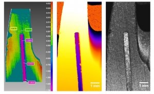
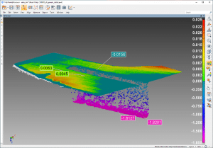
The OPTICAL 3D PROFILOMETER system comes with NOVACAM high-performance data acquisition software, which is PC Windows ® -based and user-friendly for scan programming.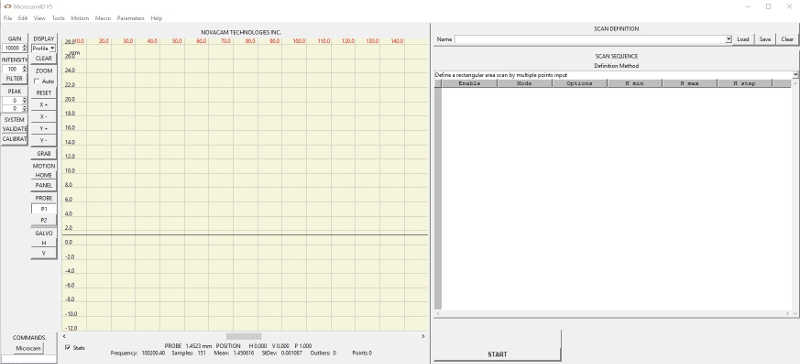 The system simultaneously generates 3 data sets from the same scan, 3D point cloud, light intensity image, and height image. The height and light intensity images facilitate defect detection. STL file format is also available.
 For full GD&T analysis of measured parts, a turnkey solution is available with PolyWorks InspectorTM , metrology software that may be purchased with the system.
- Go-no-go reporting is easily programmed and automated.
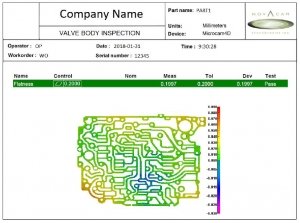
- Users benefit from capabilities such as a quick visual comparison (deviation map) of the acquired part measurements to pre-specified tolerances or to the CAD of the part.
 Visualizing the scan data may be accomplished by importing the data into various third party visualization and numerical analysis software, such as PolyWorks Inspector, Geomagic, ImageJ, SolidWorks, Octave, MatLab, Mathematica, IDL, or IGOR Pro.
Deriving application-specific measurements from the 3D point cloud is available through a selection of in-house and third party software. Novacam supports the following options:
Visualizing the scan data may be accomplished by importing the data into various third party visualization and numerical analysis software, such as PolyWorks Inspector, Geomagic, ImageJ, SolidWorks, Octave, MatLab, Mathematica, IDL, or IGOR Pro.
Deriving application-specific measurements from the 3D point cloud is available through a selection of in-house and third party software. Novacam supports the following options:
Additional Info
Standard system configuration
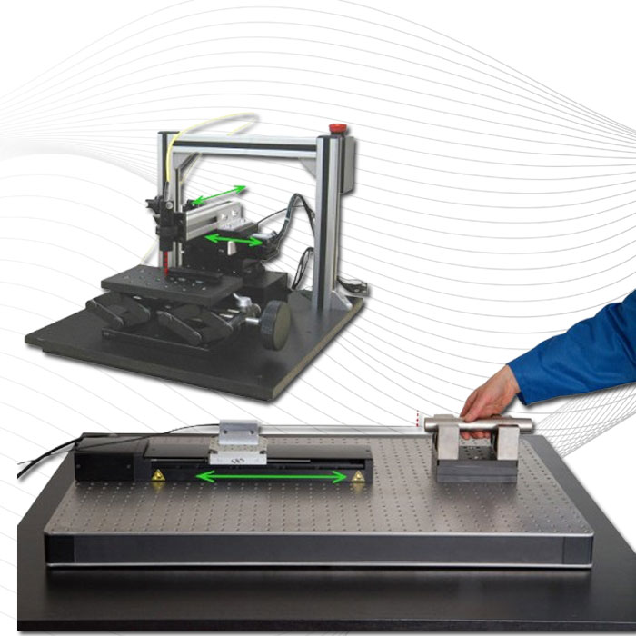
A standard configuration of the OPTICAL 3D PROFILOMETER system includes:- MICROCAM-3D interferometer
- Choice of
- 1 standard ⌀17.8 mm forward-looking probe
- OR
- 1 standard ⌀4.6 mm side-looking probe (for ID up to 300 mm (12″) deep)
- 2-axis inspection station and 2-axis motion controller
- Manual adjustment of probe height
- PC with NOVACAM acquisition software
- 1 year warranty
Instrument safety
- MICROCAM systems feature an in-probe red laser pointer (650 nm wavelength) for alignment purposes.
- MICROCAM systems are Class 1M Laser products, with < 20 mW of infrared and < 5 mW of in-probe laser pointer.
FAQ
What is the advantage of using a non-contact vs. contact profilometer for roughness measurement?
- Non-contact roughness measurements systems offer important advantages over contact measurement systems:
-
- no risk of affecting the surfaces as frequently happens with contact probe styluses
-
- no need for expensive consumables – optical probes do not get used up in the process of measuring
- no need for costly stoppages to exchange worn out contact probes.
- Yes. The scanning sequence (recipe) can be programmed with a joystick and can be recalled at later times with the push of a button.
- Yes. The system is ideally suited to both lab and shop floor inspection. Inline and robot setups are an option. The non-contact probes can even be configured to work in hostile environments such as extremely hot, cryogenic, or radioactive.
- Yes.
- Yes, depending on the geometry of the features to be scanned. Various curved surfaces and high-aspect ratio features have been scanned. Displacement stages can be added to the setup if required.
- Yes, if the coating is semi-transparent to infrared light and has optical thickness of 20 µm or higher (optical thickness = physical thickness * index of refraction).